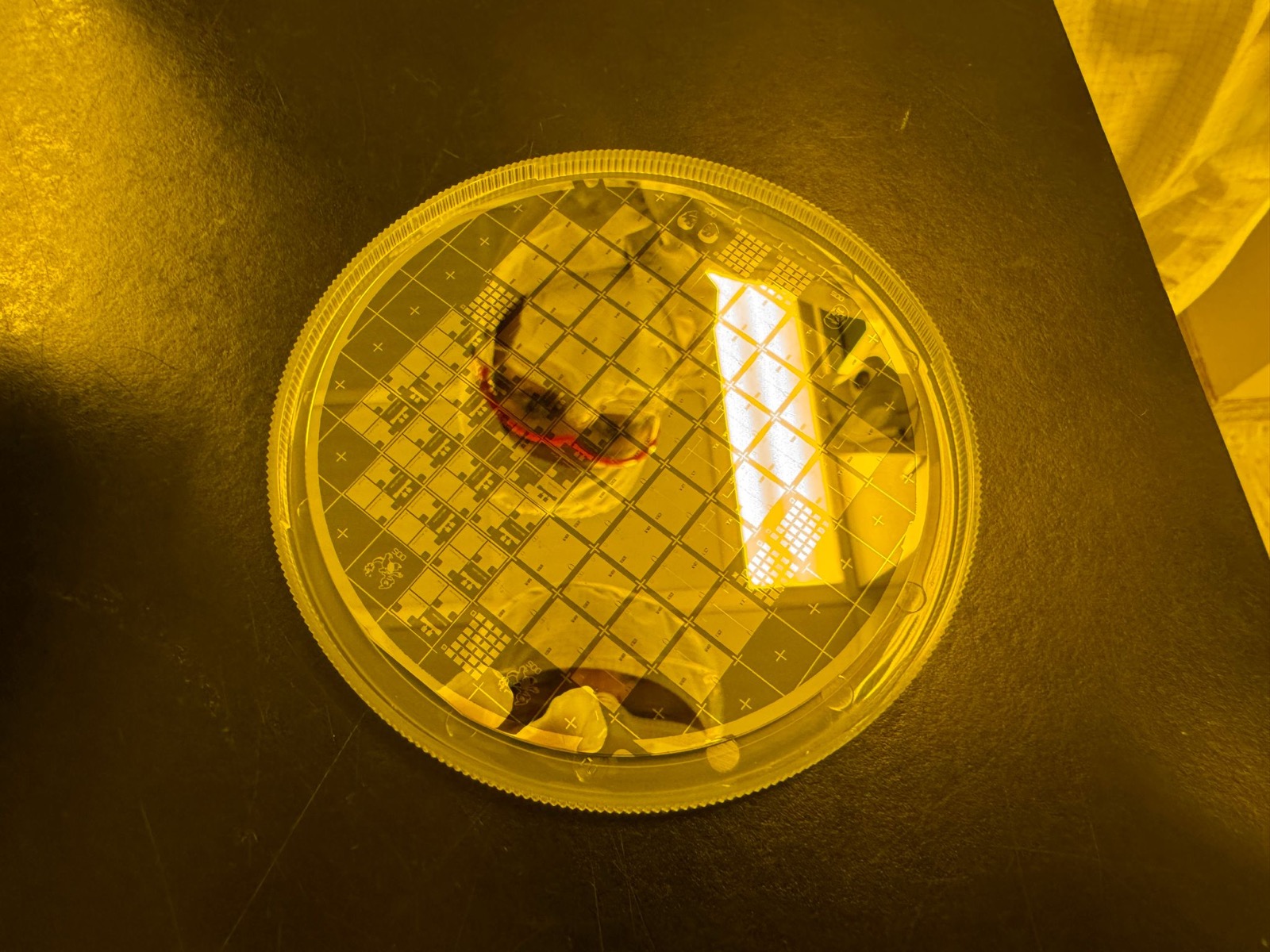
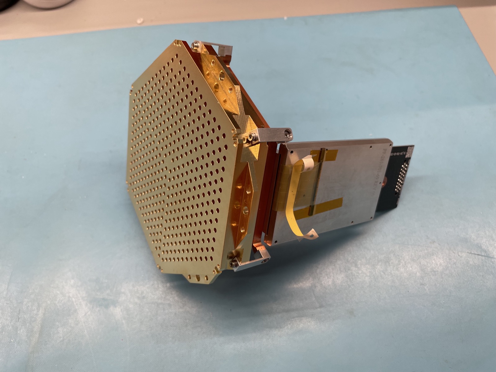
Devices
At a few hundred channels, an instrument is limited by how good its best devices are. At tens of thousands, it is limited by how alike they are. A transition-edge sensor whose critical temperature sits 10 mK from its neighbours needs a different bias point. A resonator whose frequency lands 200 kHz from where the design put it collides with the channel next to it and both are lost. Neither failure shows up when you measure one device carefully; both decide whether a multiplexed array reads out at all.
So the quantities that matter are distributions rather than single-device figures of merit: the spread in transition temperature across a wafer, the scatter in resonator frequency placement against design, and the yield that survives both. Fabrication is where those distributions are set, which makes it part of the physics rather than a service supplied to it.
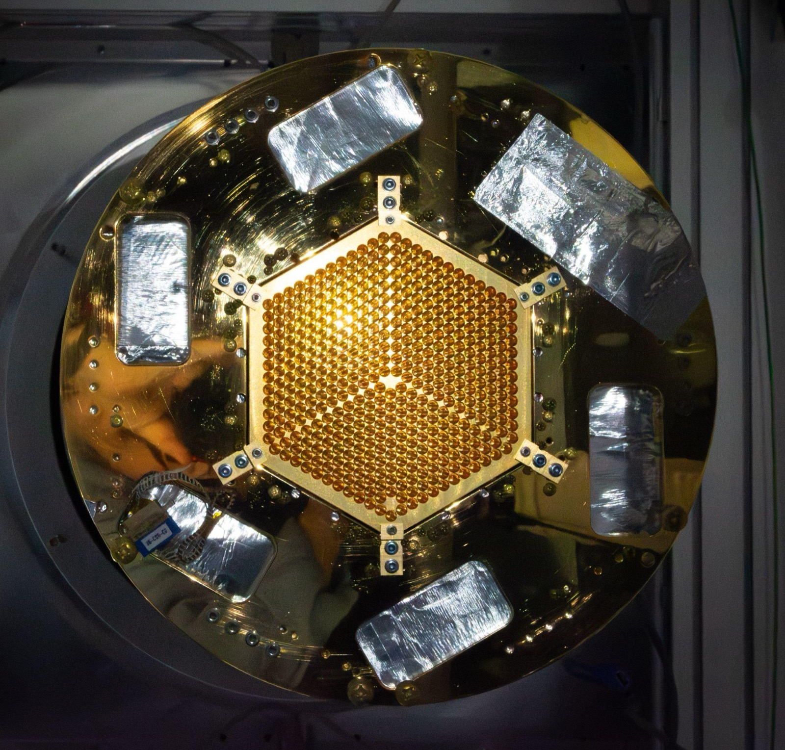
The Detector Microfabrication Facility
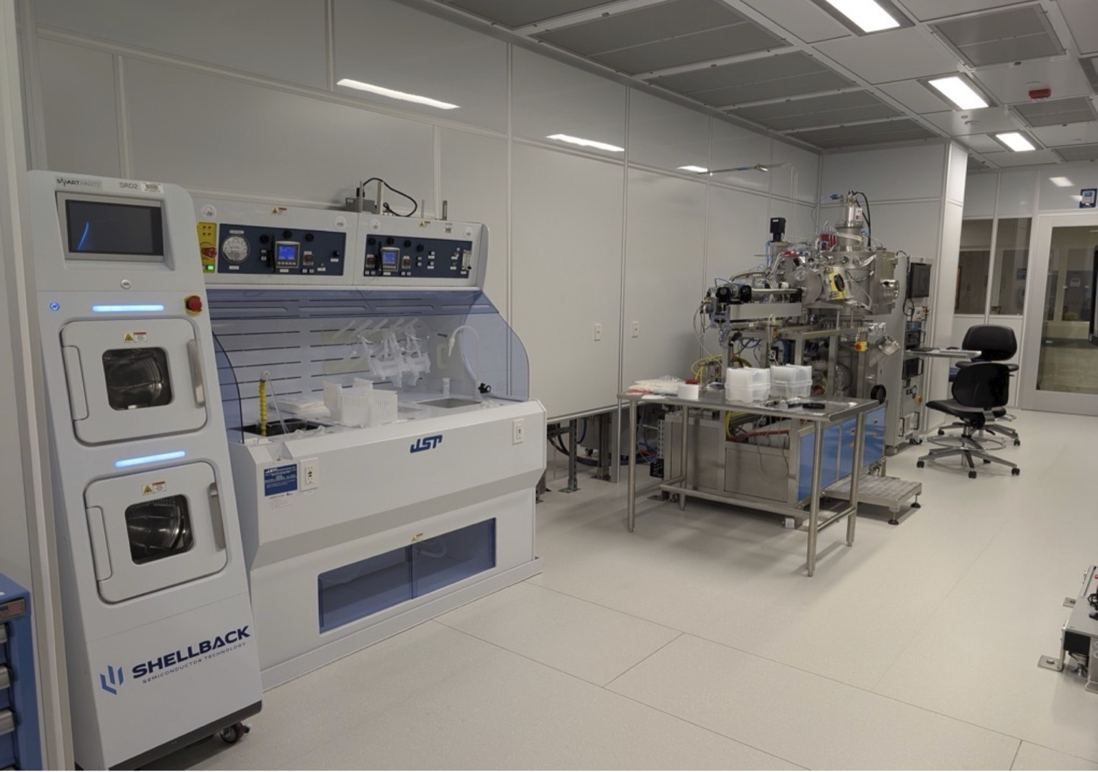
From 2022 to 2025 I directed the project that designed and built SLAC’s Detector Microfabrication Facility. The facility is now in operations, and I work in it as a principal investigator, fabricating devices for cosmology and quantum sensing. I also sit on its process review committee.
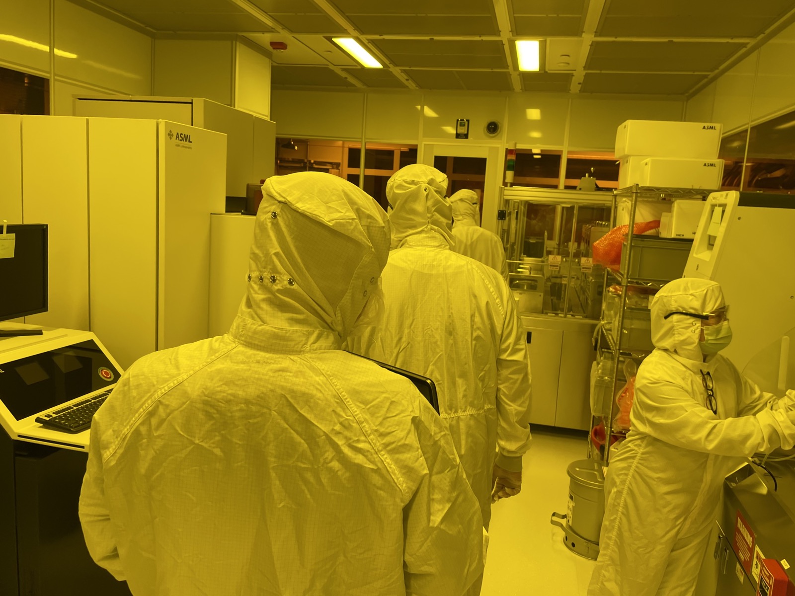
It is a 5,500 square foot Class-100 cleanroom built for 150 mm wafers, with a process line covering niobium, aluminum, and silicon oxides and nitrides. That materials set is chosen: it is what superconducting resonators, transition-edge sensors and nanowire detectors are actually made from, and having the full line in one place means a design change can be tested in weeks rather than negotiated across institutions over months.
What we make there
Superconducting nanowire single-photon detectors for the Q-NEXT photon sensors project, aimed at entanglement distribution: high detection efficiency and low timing jitter at telecom wavelengths, where the requirement is not a single good detector but many detectors whose timing behavior matches.
High kinetic inductance thin films for parametric amplification, sensing, and quantum information, under an LDRD program running 2027 to 2029. The same film platform supports low-threshold detectors for dark matter and rare-event searches, where the relevant figure of merit is how little energy can be detected at all.
What these have in common is that the limit is set by uniformity across many devices rather than by one good device, and that each of them has to be read out at scale by the SMuRF platform.